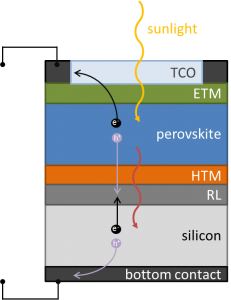
In order to make use of the current produced in a solar cell, one needs electrodes and cables to transport the produced charge carriers to the consumer – but how do the charge carriers reach the electrodes? In many solar cell types, a conductive material is necessary. As the sunlight still needs to reach the absorber layer (where the energy-transfer from photons to electrons and thus the generation of the charge carriers happens), this material not just needs to be conductive but also transparent in a wide wavelength range. This difficult task is taken over by Transparent Conductive Oxides (TCOs).
Metal oxides have shown to be suitable candidates for TCOs. Next to solar cells they are used in a lot of other applications such as flat panel displays, touch screen panels, transparent heaters and electronics, LEDs and flexible optoelectronic devices. Thus they are a very relevant topic in today’s research.
Currently the most commonly used TCOs for thin film solar cells are ITO (indium tin oxide, In2O3:Sn), IZO (indium zinc oxide, In2O3:Zn) and AZO (aluminum zinc oxide, ZnO:Al).
(not to scale).
For some solar cells another important requirement appears, e.g. for tandem solar cells. Here, the TCO needs to be deposited on top of the absorber materials, forming the so called window layer.
Due to the temperature sensitivity of some materials, perovskites for instance, the TCO needs to be deposited at low temperatures (room temperature would be ideal). Additionally, it either has to show good conductivity and transparency in the as-deposited, amorphous form or it must be possible to crystallize it at low temperatures, thereby improving its conductivity. New materials such as metal-doped indium oxides have gained attention because they require only low annealing temperatures.
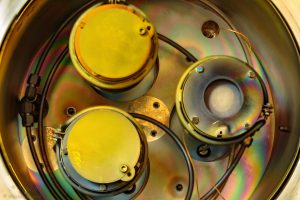
In my project I create window layers of the TCO material In2O3:W,H (indium oxide doped with tungsten and hydrogen, the doping with hydrogen promises a higher conductivity plus transparency) with the physical vapor deposition technique of magnetron sputtering. I characterize the layers using Hall-measurements for electrical properties, X-ray diffraction (XRD) for solid state phase analysis and UV/VIS-measurements for optical properties. In the deposition process I change parameters, such as the oxygen and hydrogen partial pressure in the sputter chamber, and examine their influence on the optical, electrical and structural properties of the layer.
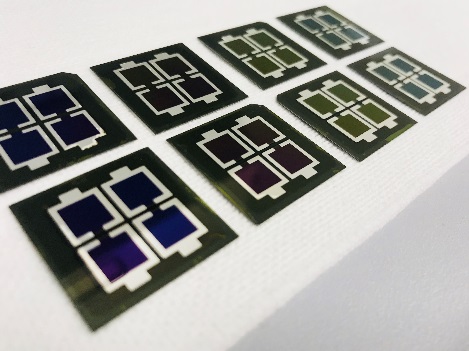
The goal of my work is to improve the efficiency of solar cells, in this case specifically of monolithic perovskite/silicon tandem solar cells. Currently the highest scientifically published efficiency for such a solar cell is reported by HZB’s young investigator group of Prof. Steve Albrecht, it reaches 26.0%.
With an improved TCO the efficiency can be further increased and better solar cells can be made. I am glad that I can contribute to this. I hope that in the future only sustainable energy sources are used providing a cheap, working and comfortable replacement to fossil fuels with whose use we destroy our planet!
Well written, and good pictures. I would just suggest starting with your very last paragraph (where you explain your motivation) instead of jumping directly into your subject. 😉