My summer research project is Optimizing Buried Junction Cubic and Orthorhombic SnS Photocathodes. For many years my research group have been searching for semiconductors and solar absorber materials that are non-toxic, abundant, stable, which crystallize at low temperature and are fabricated at low cost, but also have favorable optical and electrical properties for solar energy conversion.
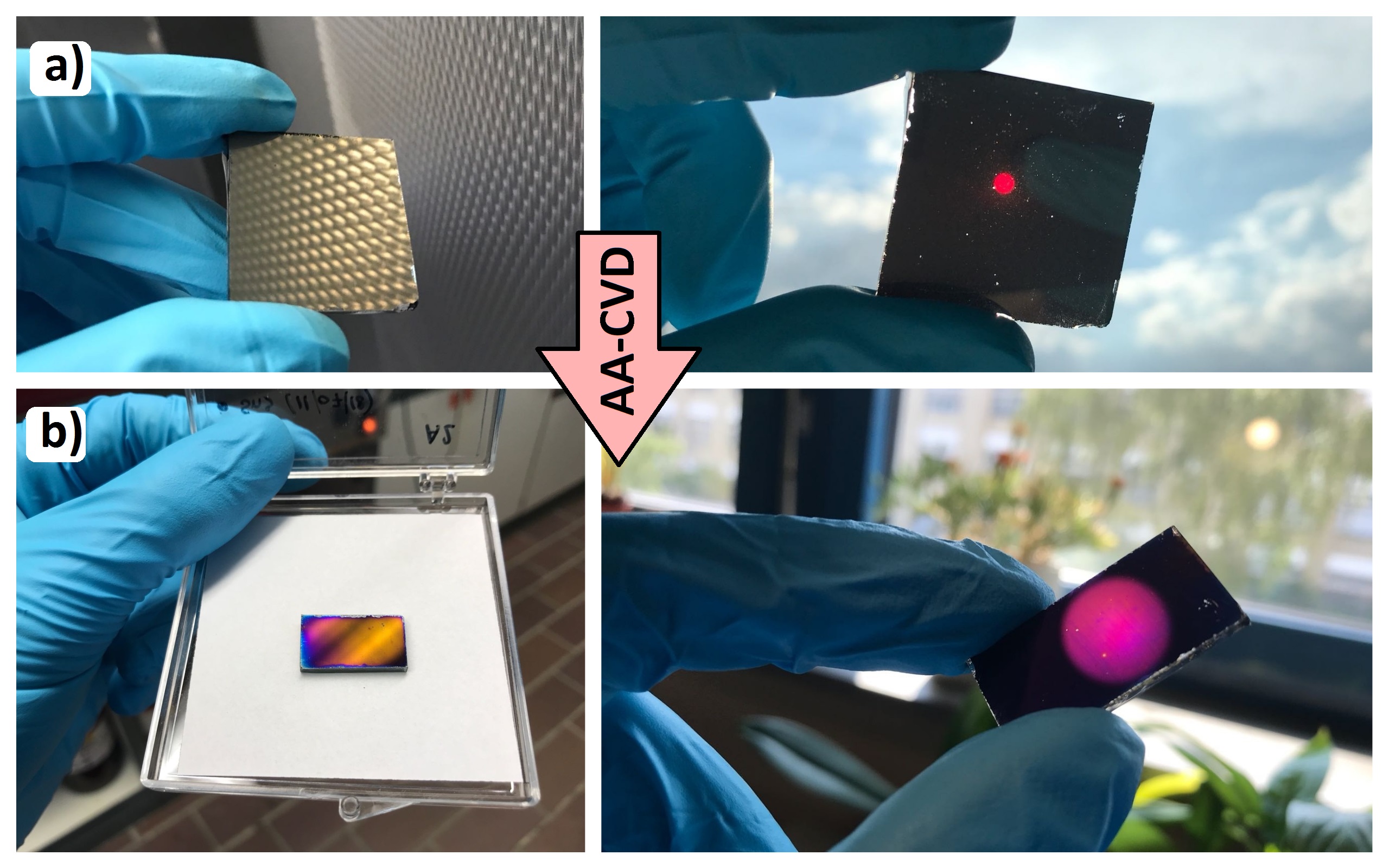
Figure 1: π-SnS photocathodes a) before and b) after coating with a passivation and protection layer.
When designing a system for solar water splitting it has been proposed that an idealized tandem device, consisting of two semiconductors with band gaps around 1.0 to 1.3 eV and 1.6 to 2.0 eV, will provide both the optimal photocurrent and photovoltage for high efficiency solar water splitting. Interestingly, it has been discovered that the earth abundant semiconductor SnS can possess two different polymorphs at room temperature; one being the metastable cubic π-SnS phase with a direct band gap of 1.7 eV, and the other being α-SnS ground state with an indirect band gap of 1.1 eV, in which both are native p-type semiconductors.
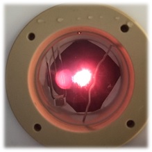
Figure 2: Measuring the PEC properties of π-SnS photocathodes under 1 sun illumination.
Here at the Institute for Solar Fuels my research group has been able to deposit highly crystalline thin films of both polymorphs with exceptional control and selectivity. Our initial investigations of these samples have shown that relatively high saturated photocurrents for hydrogen evolution can be achievable, reaching ~8 mAcm-2 at -0.3 VRHE under AM 1.5 illumination for the π-SnS phase.
My aim is to design surface treatment methods and screen protection layers/catalysts that can enhance the onset potential, passivate the surface and improve the stability of cathodic photocurrents for the π-SnS photo absorbers. These protection layers/catalysts have been deposited by AA-CVD methods. We have already begun to screen a series of protection layers, which are only 40-60 nm thick! I have been able to learn these new experimental techniques to not only fabricate thin film absorber and protection layers, but also a range of photo-electrochemical (PEC) characterization methods. We are making progress and it is extraordinary to see how such a thin layer of material on the surface of the photocathode can dramatically effect the water splitting performance of our devices.
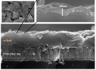
Figure 3: Scanning Electron Microscopy (SEM) images of the π-SnS photocathodes with protection/passivation layers on top.
What experimental data (tables, graphs, characteristics of the material structure, sweep, etc.) are obtained?
We have obtain light and dark CVs, stability measurements, Electrochemical impedance spec, etc, as well as teraherz spectroscopy data which gives us information about the photogenerated charge carrier diffusion lengths of the principle absorber layers. Unfortunately we are unable to disseminate these types of data via a Blog Post since this will be reserved for a future Scientific Publications.
However, you may obtain the crystallographic structure of this particular material from already published articles (e.g. https://pubs.rsc.org/en/content/articlelanding/2016/ce/c6ce00647g#!divAbstract)
I suggest to create the multifacor calculation model of your experimental data for future publication.
Dear Anton! In my profession, I am a journalist. On your page, I saw interesting information about your research with photos. And I have this question: can you tell us in an accessible language about the practical benefits of your work? Thanks for your reply!
Good afternoon, Anton,
my name is Yuan Yuan, I am from Chengdu City, Sichuan Province, China.
Your topic is very promising. In China, this problem is currently being addressed by leading universities. Do you cooperate with Chinese scientists? I will be happy to help you in establishing contacts with your Chinese colleagues.
Dear Yuan Yuan,
Thank you for your interest in our research and it is great that these subjects of investigation are being addressed on an international level.
I am glad you would like to help by facilitating collaborations, but we are reluctant to discriminate any healthy collaboration towards our Chinese colleagues only (of which none are working on this particular project), maybe you would like to form a collaboration with other colleagues?
Hello, Anton!
Have you conducted a study of your sample under conditions of electric field strength? The results of the research can be applied in the development of an optical current transformer for SmartGrid. A photocell can be used as an energy source to power a current sensor through an optical fiber on a high-voltage line. If we give the protective surface the deformation property of the current, then the element can be a current sensor.
Hello, Anton!
I like independence and initiative in your approach to scientific research. With what particular scientific sources did you work?Where, from your point of view, is it most effective to use light absorber? In what do you see the main problems and difficulties in the practical application of the results of your project? Good luck to you!
Anton, it is felt that you’re deeply interested in the theme of your research. I see, you and your group have progressed in it too. I wonder, what are the future trends (prospects) of using the results of your research? In what devices and for what purposes can this thin crystalline films find their application? I wish you further achievements in your studies.
Thank you for your question!
Overall, the goal is to fabricate a solar water splitting device that produces hydrogen.
A central component of a solar fuel device is the light absorber: a semiconductor capable of generating charge carriers upon sunlight illumination. Our efforts in the development of novel light absorbers into working solar fuel device.
I really enjoyed your post, Anton! Well done. I was wondering, what properties of your protection layers are you looking at with these photo-electrochemical (PEC) characterization methods?
We are observing the effects of improved stability, higher current densities for hydrogen evolution and optimised onset potential/photovoltage.