
By summerstudent María José Oyola Torres >
When I mention my research, people often ask about the process of making a solar cell. Before coming to HZB, I had experience fabricating solar cell devices in gloveboxes in both Colombia and Spain. I usually skip over the part where almost everything happens inside a nitrogen-filled glovebox.
Not literally me inside the box, of course — Just my arms. But this time, I will explain:
Most of the process takes place in the glovebox. This is a controlled environment, where oxygen and humidity are extremely low. That’s because we’re working with a highly sensitive semiconductor called perovskite. The glovebox also serves as a safety barrier, since the commonly used perovskite formulation contains lead, which, as you might guess, is toxic. Some very cool researchers are also working on less harmful chemical compositions, but lead perovskite solar cells are far more efficient.
Since I have to deal with lead, I must be careful to avoid direct contact or contamination with this material. Using the glovebox has become a part of my daily routine. But if, for any reason, you ever need to use one, be careful with the atmosphere when putting materials inside. Otherwise, you’ll spend time (and a lot of nitrogen) fixing it. You’ll also get some unexpected motor-skill training, and the occasional hand cramp if the gloves have wrinkles.
Now, at HZB, I’m evaluating how different surface treatments with Self-Assembled Monolayers (SAMs) affect charge transport in the device. These ultra-thin SAM layers help charge carriers move efficiently from the semiconductor to the electrodes, which ultimately increases the device’s performance.
31 nm layers and teamwork
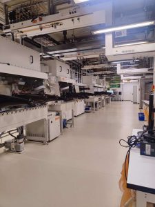
Back in the lab, at first, it felt like just switching locations. A new glovebox, slightly different spin-coating settings, but the same principles apply, whether in Colombia, Spain or Berlin. Resilience is key, both for solar devices and researchers.
That day at HZB, I was making my second batch and was almost done. I only needed to evaporate two buffer layers before heading out to meet a friend for dinner. Everything was going well until the evaporator stopped cooperating and refused to deposit the 31 nm layers.
Suddenly, a short day turned long. I stayed. I checked every parameter, repeated the process, and waited again. I asked for help, got some advice and then repeated the process, maybe four times, until we made it. It was not fun, but it was real. Sometimes you control the system, and sometimes the system controls your schedule.
Sunset
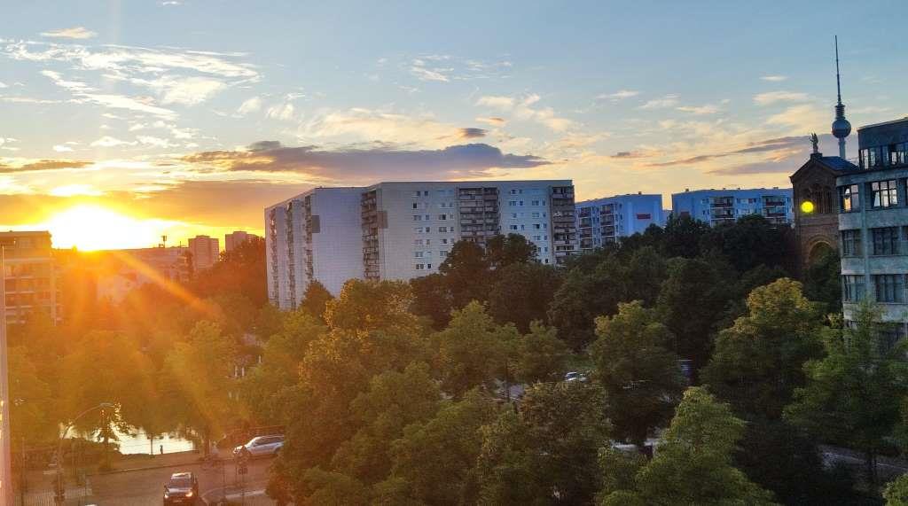
I left the lab later than planned, tired but satisfied. I had solved the problem, learned from it, explored all known strategies to fix the evaporation issue, and reached my goal.
In the end, even the frustrating parts became good stories. Since we can’t predict the future with certainty, it’s always worth remembering that when nothing goes right, go left.
About the author: María José Oyola Torres is a materials engineer from Colombia and currently a master’s student in Chemistry at the Institute of Chemical Research of Catalonia (ICIQ). During the ISSP2025 at HZB, she is working in Eva Unger’s group, evaluating how SAMs can improve the electrode/perovskite interface in solar p-i-n solar cells.